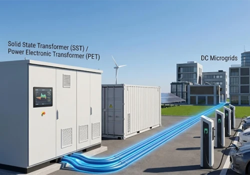




A solid‑state transformer (SST), also known as a power electronic transformer, differs from conventional line‑frequency transformers operating on 50 Hz magnetic fields. It is a controllable power conversion device composed of power electronic converters and high‑frequency transformers. Conventional line‑frequency transformers only passively transform voltage according to turns ratio. In addition to galvanic isolation and voltage conversion, SSTs provide digital‑controlled capabilities including bidirectional power flow, voltage regulation, harmonic suppression and reactive‑power compensation, serving as power routers in smart grids.
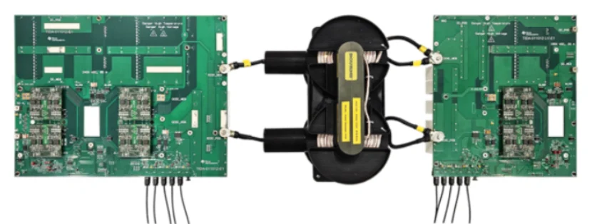
Board Setup
https://training-dev.ti.com/tool/TIDA-011012#tech-docs
Sub‑module Overall Architecture
Each sub‑module consists of two major hardware sections: an AC‑DC high‑voltage conversion unit and a DAB high‑frequency isolated DC‑DC unit. For medium‑voltage grid applications such as 10 kV systems, multiple sub‑modules are connected in series at their AC‑side terminals to share the total grid voltage. Each sub‑module owns an independent intermediate DC‑link, which is galvanically isolated from others with no DC‑voltage stacking. All low‑voltage DC outputs of DAB converters are connected in parallel to form a unified low‑voltage DC bus.
|
Important characteristic: No matter how many sub‑modules are connected in series, the intermediate DC‑link voltage of each individual sub‑module remains at its nominal value. Series‑connected AC terminals only divide the grid‑frequency AC voltage. Each sub‑module implements independent closed‑loop voltage regulation, so its internal DC‑link will not rise along with the total grid voltage. Fiber‑optic communication is adopted for control signals between high‑potential and low‑potential domains to avoid interference and breakdown risks caused by floating high‑voltage potentials. |
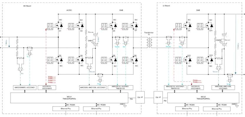
Block Diagram
https://training-dev.ti.com/tool/TIDA-011012#tech-docs
Stage 1: Bidirectional H‑bridge AC‑DC Conversion
The input‑side single‑phase H‑bridge consists of four SiC power switches, boost inductors and DC‑link capacitors, implementing a bidirectional Boost‑PFC topology operating at kilohertz‑level switching frequency. It supports both rectification and reverse grid‑tied inversion.
In rectification mode, the sub‑module receives divided grid‑frequency AC voltage. High‑speed PWM switching of H‑bridge switches cooperates with boost inductors to store and release magnetic‑field energy, converting grid‑frequency AC into stabilized intermediate DC‑link voltage. This stage also realizes power‑factor correction, ensuring sinusoidal grid‑side current and harmonic suppression. It should be noted that the DC‑link voltage must exceed the peak value of input AC voltage to satisfy boost‑operation conditions.
During reverse‑power operation, the H‑bridge works as an inverter. It converts energy stored on the intermediate DC‑link back into grid‑frequency AC injected into the utility grid. Reactive‑power output is also achievable for grid power‑quality regulation.
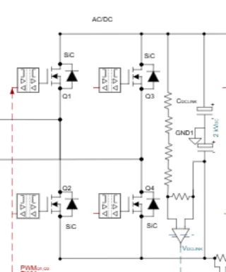
AC‑DC Conversion
|
Key System Specifications of the DC/AC Converter |
||
|
Parameters |
Specification |
Details |
|
Nominal AC Power |
±50kVA |
± Active ± Reactive |
|
Nominal AC Voltage |
1000 VRMS |
|
|
Nominal AC Current |
50 ARMS |
|
|
Nominal DC Voltage |
2200VDC |
|
|
DC Link Voltage Ripple |
±200V |
at 2200V |
|
Switching Frequency |
From 5kHz to 10kHz |
H-Bridge Unipolar |
|
Cooling Technology |
Air Force Cooling |
12V Fans |
|
Max Ambient Temperature |
60°C |
|
|
Power FETs Specs |
3.3kV, 22.5mΩ |
SiC FETs |
Stage 2: DAB Dual‑Active‑Bridge High‑Frequency Isolated DC‑DC Conversion
As the isolation core of the sub‑module, the DAB comprises a primary‑side full‑bridge, a high‑frequency transformer and a secondary‑side full‑bridge. It operates at hundreds of kilohertz with native bidirectional‑power capability.
Primary‑side full‑bridge inversion: Drawing energy from the preceding H‑bridge intermediate DC‑link, SiC switches chop DC voltage into high‑frequency AC square waves whose amplitude equals the DC‑link voltage, feeding the primary winding of the high‑frequency transformer. Transformers cannot conduct DC current; only alternating square‑wave voltage establishes alternating magnetic fields inside the core for energy transfer. High‑frequency operation enables smaller transformer cores and permits zero‑voltage‑switching (ZVS) to reduce switching losses.
High‑frequency transformer for voltage transformation and galvanic isolation: Fed by high‑frequency square waves, the transformer alters voltage amplitude according to its winding turns‑ratio and provides complete galvanic isolation between high‑voltage primary and low‑voltage secondary domains. Voltage conversion ratio is determined by transformer turns‑ratio rather than phase‑shift control. The intrinsic leakage inductance of the transformer is utilized as the series power‑transfer inductor for the DAB.
Secondary‑side full‑bridge active rectification: The secondary‑side full‑bridge processes high‑frequency square‑wave voltage delivered by the transformer. Unlike passive diode rectification, the active full‑bridge precisely controls SiC switching timings. Whether the square‑wave is in positive or negative half‑cycle, alternating AC energy is converted into charging current for output capacitors. Output capacitors filter high‑frequency ripples and produce smooth low‑voltage DC output.
For reverse‑power flow, the secondary‑side full‑bridge acts as an inverter, chopping low‑voltage DC back into high‑frequency square‑waves sent to the transformer secondary. Energy is boosted by the transformer, then reconstructed into intermediate DC voltage by the primary‑side full‑bridge.
The DAB adopts single‑phase‑shift (SPS) control. Both primary‑ and secondary‑side full‑bridges generate 50 %‑duty‑ratio square‑wave waveforms. The controller adjusts the phase‑angle difference between the two sets of waveforms. Phase‑shift magnitude controls transmitted‑power magnitude, and phase‑shift polarity determines power‑flow direction. Phase‑shift only regulates power, it cannot achieve wide‑range steady‑state output‑voltage adjustment. Forcing output voltage far away from the turns‑ratio‑matched nominal operating point will lose ZVS conditions, introduce heavy circulating current and cause severe device overheating. To change the rated output voltage, the high‑frequency transformer turns‑ratio must be redesigned.
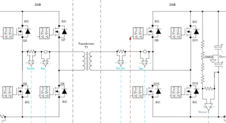
DAB
|
Key System Specifications of the DC/DC Converter |
||
|
Parameters |
Specification |
Details |
|
Nominal DC Power |
±50kW |
Bidirectional Power Flow |
|
MV Nominal DC Voltage |
2.2kV |
|
|
MV Nominal DC Current |
23A |
|
|
LV Nominal DC Voltage |
1.5kV |
|
|
LV Nominal DC Current |
33.3A |
|
|
Switching Frequency |
100kHz |
|
|
Max Ambient Temperature |
60°C |
|
|
Power FETs Specs on MV |
3.3kV, 22.5mΩ |
SiC FETs |
|
Power FETs Specs on LV |
2.3kV, 11.5mΩ |
SiC FETs |
System Scaling and Engineering Constraints
In medium‑voltage high‑power applications, voltage and power scaling are realized by multiple sub‑modules with series‑connected AC inputs and parallel‑connected DC outputs. The common low‑voltage bus voltage of paralleled sub‑modules is locked by DAB transformer turns‑ratio. When target output voltage deviates from the intrinsic DAB output voltage, two practical solutions exist:
Retain original hardware and add an extra non‑isolated DC‑DC converter for post‑regulation step‑down;
Redesign the high‑frequency transformer, re‑verify component stress and retune control algorithms for deep DAB modification.
|
Forward‑direction power‑conversion chain summary: |

Why SST Achieves Compact Size
Conventional distribution transformers work at 50 Hz line frequency and require large magnetic‑core cross‑sectional area to deliver rated power. According to electromagnetic principles: for a given power rating, higher operating frequency reduces the required core volume and weight.
Instead of driving the isolation transformer directly with 50 Hz mains voltage, SST power electronics convert grid‑frequency power into hundreds‑kHz high‑frequency square‑wave voltage feeding the high‑frequency isolation transformer. Compared with line frequency, the operating frequency increases by thousands of times, so the volume and weight of high‑frequency magnetic components can be reduced by more than ten‑fold.
N = k * 10^5 * U / (f * Ae * Bmax )
k - Ratio of maximum on-time to switching period, typically k=0.4;
U - Primary winding input voltage (V), approximately equal to DC input voltage;
f - Operating frequency of transformer (kHz);
Ae - Effective cross-sectional area of magnetic core (cm²);
Bmax - Maximum allowable swing of magnetic flux density (G).

Inherent Drawbacks
Large‑quantity semiconductor devices bring high hardware complexity and higher cost compared with conventional transformers. High‑frequency switching produces electromagnetic interference (EMI), imposing strict requirements on PCB layout, magnetic‑component design and thermal management. Therefore SST will not fully replace line‑frequency transformers, and is mainly applied in new‑power‑system scenarios demanding compact footprint, bidirectional‑power flow, DC interfaces and active power‑quality control.