


Gallium doping is a method for preventing light induced degradation (LID), particularly in PERC cells. Using Ga-doped silicon wafers for solar cell application definitely results in better performance of solar cells and PV modules, as well as the improvement of their long-term reliability.

Schematic diagram of PERC solar cell
According to the press statement, Shin-Etsu Chemical holds several patents on gallium doping in silicon crystals and on using gallium-doped p-type crystalline silicon wafers in the production of photovoltaic (PV) cells.
It is widely known that solar cells that make use of boron-doped p-type silicon wafers suffer from light induced degradation (LID). This occurs in the very first hours that the crystalline p-type boron doped silicon solar cells are exposed to the sun, causing a loss of performance and a general degradation of conversion efficiency.

This LID is associated with the formation of the boron oxygen complex, which acts as a harmful defect and reduces the minority carrier diffusion length. Although lots of research has gone into the characterisation and mitigation of LID to date, industrial solar cells still suffer from different types of light-induced efficiency losses.
Using gallium doping to prevent LID
However, there is an industrial alternative to boron doped silicon—gallium doped silicon. It is thought to be immune from LID, particularly when it is used in PERC cells.
In October 2019, a Chinese-based company, JA Solar, was awarded intellectual property rights for its own gallium doping technology that is used in photovoltaic (PV) cell production. JA Solar explained that its proprietary technology can effectively mitigate the LID effect on PV modules that are assembled with p-type silicon wafers.
"Using Ga-doped silicon wafers for solar cell application definitely results in better performance of solar cells and PV modules, as well as the improvement of their long-term reliability,” said chairman and board of directors Jin Baofang.
The company also holds several patents on gallium doping in silicon crystals and on using gallium-doped p-type crystalline silicon wafers in the production of PV cells.
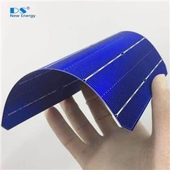
Ga doped silicon solar wafer
Ga doped silicon solar wafer 210mm M12 G12
Ga doped silicon solar wafer 166mm M6
Ga doped silicon solar wafer 161.7mm M4
Ga doped silicon solar wafer 158.75mm G1 full square
Ga doped silicon solar wafer 156.75mm M2