









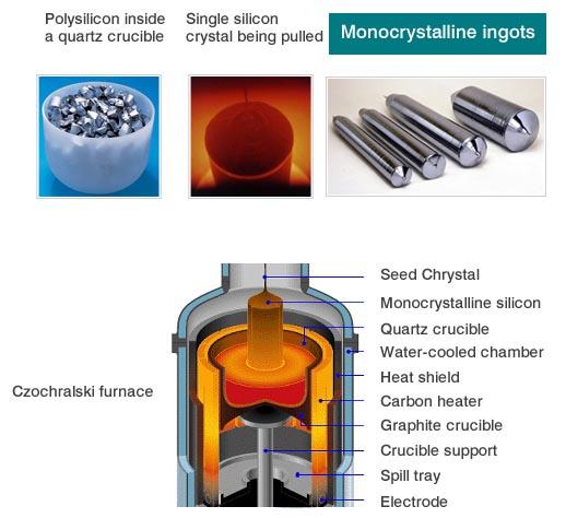
Czochralski (CZ) Process for Monocrystalline Silicon Production
Crafted with premium Czochralski growth and phosphorus doping, N-Type M12 monocrystalline silicon wafer comes in 210×210mm large pseudo square size to expand light-receiving area and upgrade module power generation efficiency. It boasts low dislocation density, stable resistivity and ultra-long minority carrier lifetime, paired with precise dimensional accuracy and superior surface finish. Fully adaptable to HJT, TOPCon and other advanced cell processes, it is an ideal base material for manufacturing high-efficiency and high-power photovoltaic modules.
Core Features & Application Advantages
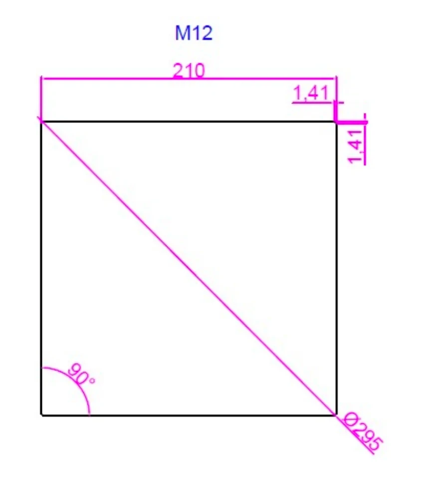
The N-Type M12 Monocrystalline Silicon Wafer adopts a large pseudo square 210×210 mm format (φ295 mm diameter), increasing the active area and boosting power output for high-efficiency PV modules. Grown using the CZ method and doped with phosphorus, it features a <100> surface orientation, low dislocation density (≤500 cm⁻²), and N-type conductivity. With a resistivity range of 1.0–7.0 Ω·cm and minority carrier lifetime ≥1000 µs, it is ideal for advanced solar cell technologies such as TOPCon and HJT. The M12 wafer's optimized geometry and surface quality ensure excellent performance in next-generation high-power modules.

Material properties
| Property | Specification | Inspection Method |
| Growth method | CZ | |
| Crystallinity | Monocrystalline | Preferential Etch Techniques(ASTM F47-88) |
| Conductivity type | N-type | Napson EC-80TPN |
| Dopant | Phosphorus | - |
| Oxygen concentration[Oi] | ≦8E+17 at/cm3 | FTIR (ASTM F121-83) |
| Carbon concentration[Cs] | ≦5E+16 at/cm3 | FTIR (ASTM F123-91) |
| Etch pit density(dislocation density) | ≦500 cm-2 | Preferential Etch Techniques(ASTM F47-88) |
| Surface orientation | <100>±3° | X-ray Diffraction Method (ASTM F26-1987) |
| Orientation of pseudo square sides | <010>,<001>±3° | X-ray Diffraction Method (ASTM F26-1987) |
Electrical properties
| Property | Specification | Inspection Method |
| Resistivity | 1.0-7.0 Ω.cm | Wafer inspection system |
| MCLT (minority carrier lifetime) | ≥1000 µs | Sinton BCT-400Transient(with injection level: 5E14 cm-3) |
Geometry
| Property | Specification | Inspection Method |
| Geometry | pseudo square | |
| Bevel edge shape | round | |
| Wafer Side length | 210±0.25 mm | wafer inspection system |
| Wafer Diameter | φ295±0.25 mm | wafer inspection system |
| Angle between adjacent sides | 90° ± 0.2° | wafer inspection system |
| Thickness | 180 ﹢ 20/﹣10 µm175﹢ 20/﹣10 µm170﹢ 20/﹣10 µm165﹢ 20/﹣10 µm160﹢ 20/﹣10 µm150﹢ 10/﹣10 µm | wafer inspection system |
| TTV (Total thickness variation) | ≤ 27 µm | wafer inspection system |
Surface properties
| Property | Specification | Inspection Method |
| Cutting method | DW | -- |
| Surface quality | as cut and cleaned, no visible contamination, (oil or grease, finger prints, soap stains, slurry stains, epoxy/glue stains are not allowed) | wafer inspection system |
| Saw marks / steps | ≤ 15µm | wafer inspection system |
| Bow | ≤ 40 µm | wafer inspection system |
| Warp | ≤ 40 µm | wafer inspection system |
| Chip | depth ≤0.3mm and length ≤ 0.5mm Max 2/pcs; no V-chip | Naked eyes or wafer inspection system |
| Micro cracks / holes | Not allowed | wafer inspection system |
Hot Tags: n-type m12 monocrystalline silicon wafer specification, China, suppliers, manufacturers, factory, made in China


