





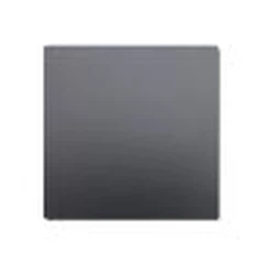
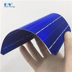


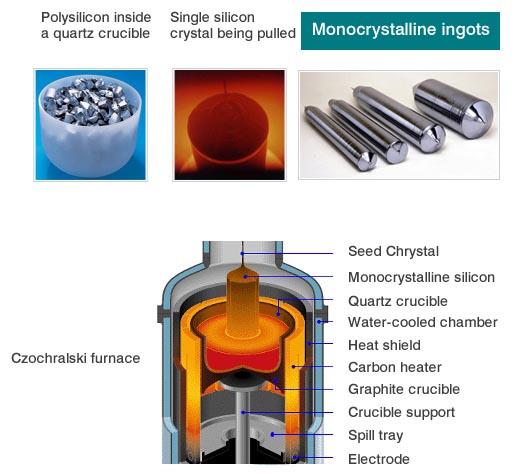

The N-Type G1 Monocrystalline Silicon Wafer features a full square 158.75×158.75 mm design, maximizing light exposure and module efficiency. Manufactured using the CZ method with phosphorus doping, it offers excellent material quality, low dislocation density (≤500 cm⁻²), and <100> crystal orientation. With N-type conductivity, a resistivity range of 0.5–7 Ω·cm, and carrier lifetime up to ≥1000 µs, it is well-suited for high-efficiency cell technologies like TOPCon and HJT. Its full square shape and tight geometric tolerances ensure optimal module integration and performance.
1. Material properties
|
Property |
Specification |
Inspection Method |
|
Growth method |
CZ |
|
|
Crystallinity |
Monocrystalline |
Preferential Etch Techniques(ASTM F47-88) |
|
Conductivity type |
N-type |
Napson EC-80TPN |
|
Dopant |
Phosphorus |
- |
|
Oxygen concentration[Oi] |
≦8E+17 at/cm3 |
FTIR (ASTM F121-83) |
|
Carbon concentration[Cs] |
≦5E+16 at/cm3 |
FTIR (ASTM F123-91) |
|
Etch pit density(dislocation density) |
≦500 cm-2 |
Preferential Etch Techniques(ASTM F47-88) |
|
Surface orientation |
<100>±3° |
X-ray Diffraction Method (ASTM F26-1987) |
|
Orientation of pseudo square sides |
<010>,<001>±3° |
X-ray Diffraction Method (ASTM F26-1987) |
2.Electrical properties
|
Property |
Specification |
Inspection Method |
|
Resistivity |
1.0-7.0 Ω.cm
|
Wafer inspection system |
|
MCLT (minority carrier lifetime) |
≥1000 µs(Resistivity>1.0ohm.cm)
≥500 µs (Resistivity<1.0ohm.cm)
|
Sinton BCT-400
QSSPC/Transient
(with injection level: 1E15 cm -3)
|
3.Geometry
|
Property |
Specification |
Inspection Method |
|
Geometry |
pseudo square |
|
|
Bevel edge shape
|
round | |
|
Wafer Side length |
182±0.25 mm
|
wafer inspection system |
|
Wafer Diameter |
φ247±0.25 mm |
wafer inspection system |
|
Angle between adjacent sides |
90° ± 0.2° |
wafer inspection system |
|
Thickness |
180﹢ 20/﹣10 µm
175﹢ 20/﹣10 µm
170﹢ 20/﹣10 µm
160﹢ 20/﹣10 µm
150﹢ 20/﹣10 µm
|
wafer inspection system |
|
TTV (Total thickness variation) |
≤ 27 µm |
wafer inspection system |

4.Surface properties
|
Property |
Specification |
Inspection Method |
|
Cutting method |
DW |
-- |
|
Surface quality |
as cut and cleaned, no visible contamination, (oil or grease, finger prints, soap stains, slurry stains, epoxy/glue stains are not allowed) |
wafer inspection system |
|
Saw marks / steps |
≤ 15µm |
wafer inspection system |
|
Bow |
≤ 40 µm |
wafer inspection system |
|
Warp |
≤ 40 µm |
wafer inspection system |
|
Chip |
depth ≤0.3mm and length ≤ 0.5mm Max 2/pcs; no V-chip |
Naked eyes or wafer inspection system |
|
Micro cracks / holes |
Not allowed |
wafer inspection system |
Hot Tags: n-type g1 monocrystalline silicon wafer specification, China, suppliers, manufacturers, factory, made in China


