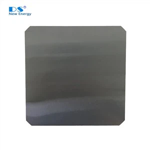
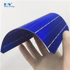

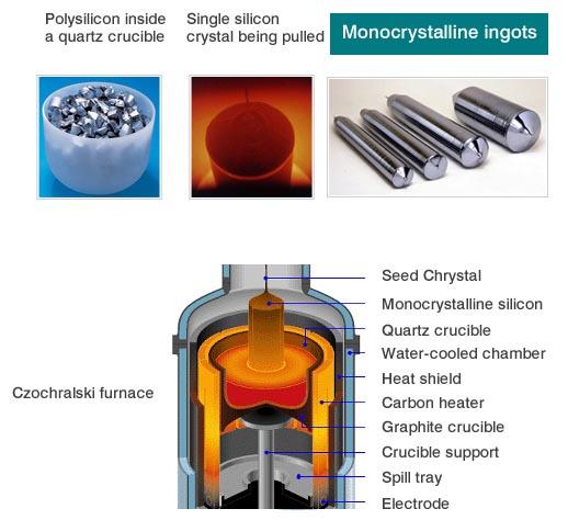

In solar PV industry, wafer technology transition comes a shift from pseudo square 156.75x156.75mm M2 to larger wafer sizes at full square 158.75x158.75mm and this includes p-type and n-type mono-Si wafers.
The state-of-art Full Square Mono Wafers have maximized the light exposure to the same level of multi wafer by expanding the square measure. The wafers are always fully square so that they fit the PV module in an optimal way.
1Material properties
Conductivity type
N-type
Napson EC-80TPN
Dopant
Phosphorus
-
Oxygen concentration[Oi]
≦8E+17 at/cm3
FTIR (ASTM F121-83)
Carbon concentration[Cs]
≦5E+16 at/cm3
FTIR (ASTM F123-91)
Etch pit density(dislocation density)
≦500 cm-3
Preferential Etch Techniques(ASTM F47-88)
Surface orientation
<100>±3°
X-ray Diffraction Method (ASTM F26-1987)
Orientation of pseudo square sides
<010>,<001>±3°
X-ray Diffraction Method (ASTM F26-1987)
2Electrical properties
|
Property |
Specification |
Inspection Method |
|
Resistivity |
0.3-2.1 Ω.cm 1.0-7.0 Ω.cm |
Wafer inspection system |
|
MCLT (minority carrier lifetime) |
≧1000 μs(Resistivity 0.3-2.1 Ω.cm) |
Sinton transient |
3Geometry
|
Property |
Specification |
Inspection Method |
|
Geometry |
Full square |
|
|
Wafer Side length |
158.75±0.25 mm |
wafer inspection system |
|
Wafer Diameter |
φ223±0.25 mm |
wafer inspection system |
|
Angle between adjacent sides |
90° ± 0.2° |
wafer inspection system |
|
Thickness |
180 ﹢ 20/﹣10 µm; 170﹢ 20/﹣10 µm |
wafer inspection system |
|
TTV (Total thickness variation) |
≤ 27 µm |
wafer inspection system |

4Surface properties
|
Property |
Specification |
Inspection Method |
|
Cutting method |
DW |
-- |
|
Surface quality |
as cut and cleaned, no visible contamination, (oil or grease, finger prints, soap stains, slurry stains, epoxy/glue stains are not allowed) |
wafer inspection system |
|
Saw marks / steps |
≤ 15µm |
wafer inspection system |
|
Bow |
≤ 40 µm |
wafer inspection system |
|
Warp |
≤ 40 µm |
wafer inspection system |
|
Chip |
depth ≤0.3mm and length ≤ 0.5mm Max 2/pcs; no V-chip |
Naked eyes or wafer inspection system |
|
Micro cracks / holes |
Not allowed |
wafer inspection system |
Hot Tags: n type full square monocrystalline solar wafer, China, suppliers, manufacturers, factory, made in China