
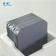
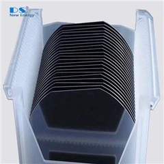


There are eight steps to produce solar cells from silicon wafers to the final testing of the ready solar cell.
Step 1: Wafer check
Silicon wafer is the carrier of solar cell. The quality of silicon wafer directly determines the conversion efficiency of solar cell, so it is necessary to test the incoming silicon wafer. This process is mainly used for online measurement of some technical parameters of silicon wafers, such as surface roughness, minority lifetime, resistivity, P/N type and microcrack, etc. The equipment consists of automatic loading and unloading, wafer transmission, system integration and four detection modules.

Among them, the photovoltaic silicon wafer detector detects the surface roughness of the silicon wafer, and at the same time detects the appearance parameters such as the size and diagonal line of the silicon wafer. The microcrack detection module is used to detect the internal microcracks of silicon wafer. In addition, there are two detection modules, one of which is online testing module mainly testing wafer resistivity and wafer type, and the other module is used to test the minority life of silicon wafer. Before the detection of minority lifetime and resistivity, the diagonal and microcrack of the silicon wafer should be detected and the damaged silicon wafer should be automatically removed. The wafer testing equipment can automatically load and unload the wafer, and can put the unqualified products in fixed position, so as to improve the testing accuracy and efficiency.
Step 2: Texturing and Cleaning

The preparation of the surface of the monocrystalline silicon suede is to use the anisotropic corrosion of silicon to form millions of four-sided pyramidal structures on the silicon surface of every square centimeter. Due to the multiple reflection and refraction of incident light on the surface, the absorption of light is increased, and the short-circuit current and conversion efficiency of the battery are improved.
Silicon anisotropic corrosion solutions are usually hot alkaline solutions. Available bases are sodium hydroxide, potassium hydroxide, lithium hydroxide, and ethylenediamine. Most of them use cheap sodium hydroxide dilute solution with a concentration of about 1% to prepare suede silicon, and the corrosion temperature is 70-85℃. In order to obtain uniform suede, alcohols such as ethanol and isopropanol should be added as complexing agents to accelerate the corrosion of silicon. Prior to the preparation of the suede, the silicon wafer shall undergo initial surface corrosion, and about 20 ~ 25 microns of alkaline or acidic corrosion liquid shall be used to remove it. After the suede is corroded, general chemical cleaning shall be carried out. The silicon wafers prepared on the surface should not be stored in water for a long time to prevent contamination.
Step 3: Diffusion

A large area of PN junction is needed to realize the conversion of light energy to electric energy. The diffusion furnace is a special equipment for manufacturing PN junction of solar cells. The tubular diffusion furnace is mainly composed of four parts: the upper part of the quartz boat, the exhaust gas chamber, the furnace body part and the gas cabinet part. Generally, the liquid source of phosphorus oxychloride is used as the diffusion source. P type silicon wafers are placed in the quartz container of tubular diffusion furnace. Phosphorus oxychloride is put into the quartz container by nitrogen at the high temperature of 850-- 900 degrees Celsius. Phosphorus oxychloride reacts with silicon wafers to obtain phosphorus atoms. After a certain period of time, phosphorus atoms enter the surface layer of silicon wafers from all around, and permeate into the silicon wafers through the gap between silicon atoms, forming the junction of n-type semiconductor and p-type semiconductor, namely the PN junction. The PN junction produced by this method has good uniformity, the unevenness of the block resistance is less than 10%, and the minority lifetime is greater than 10ms. Making PN junction is the most basic and key process in solar cell production. Because it is the formation of the PN junction, so that the electrons and holes in the flow will not return to the original, so the formation of a current, using a wire to lead out the current, is the direct current. This process is used in the production and manufacture of solar cell wafers.
Step 4: Edge Isolation & Cleaning
By means of chemical corrosion, the silicon wafers are immersed in hydrofluoric acid solution to generate a chemical reaction to form the soluble complex hexafluorosilicic acid, so as to remove a layer of phosphorous silicon glass formed on the surface of the silicon wafers after diffusion. In the diffusion process, POCL3 reacts with O2 to generate P2O5 deposition on the surface of silicon wafer. P2O5 reacts with Si to generate SiO2 and phosphorus atoms. In this way, a layer of SiO2 containing phosphorus elements is formed on the surface of silicon wafer, which is called phosphosilicon glass.
The equipment for phosphorus silicon glass is generally composed of the body, cleaning tank, servo drive system, mechanical arm, electrical control system and automatic acid distribution system, etc. The main power sources are hydrofluoric acid, nitrogen, compressed air, pure water, heat exhaust and waste water. Hydrofluoric acid can dissolve silica because hydrofluoric acid reacts with silica to form volatile silicon tetrafluoride gas. If hydrofluoric acid is excessive, the silicon tetrafluoride formed by the reaction will further react with hydrofluoric acid to form a soluble complex hexafluorosilicic acid.

Due to the process of diffusion, even if using back-to-back diffusion, all surfaces including edges of silicon wafer will inevitably be diffused with phosphorus. The photogenerated electrons collected from the front of the PN junction will flow to the back of the PN junction along the edge of the phosphorous area, causing a short circuit. Therefore, the doped silicon around the solar cell must be etched to remove the PN junction at the edge of the cell.
Plasma etching is usually used to complete this process. Plasma etching is a process in which the parent molecule of reactive gas CF4 ionizes and forms plasma under the excitation of rf power at low pressure. Plasma is composed of charged electrons and ions, the gas in the reaction chamber under the impact of electrons, in addition to transforming into ions, but also can absorb energy and form a large number of active groups. Reactive groups reach the surface of SiO2 due to diffusion or under the action of electric field, where they have chemical reactions with the surface of the etched material, and form volatile reaction products that escape from the surface of the etched material and are extracted from the cavity by the vacuum system.
Step 5: ARC (Anti-Reflective Coating) Deposition

The reflectivity of the polished silicon surface of the plated anti-reflection film is 35%. In order to reduce the surface reflection and improve the conversion efficiency of the battery, a layer of silicon nitride anti-reflection film needs to be deposited. Nowadays, PECVD equipment is often used to prepare antireflection film in industrial production. PECVD is plasma enhanced chemical vapor deposition. It is the technical principle of low temperature plasma is used as the energy source, the sample on the cathode glow discharge under low pressure, using the glow discharge heating samples up to a predetermined temperature, and then pass into the reaction gas SiH4 and NH3, gas through a series of chemical reaction and plasma, forming a solid film in the surface of the sample is silicon nitride thin films. Generally, thin films deposited by this plasma-enhanced chemical vapor deposition method are about 70nm thick. A film of this thickness is optically functional. Using the principle of thin film interference, the light reflection can be greatly reduced, the short-circuit current and output of the battery can be greatly increased, and the efficiency can also be improved.
Step 6: Contact Printing
Screen printing solar cells have been made into PN junction after lint making, diffusion and PECVD and other processes, which can generate electric current under light. In order to export the generated current, positive and negative electrodes need to be made on the surface of the battery. There are many ways to make electrodes, and screen printing is the most common process to make solar cell electrodes. Screen printing USES the method of embossing to print the predetermined graphics on the substrate.

The equipment consists of three parts: silver paste printing on the back of the battery, aluminum paste printing on the back of the battery and silver paste printing on the front of the battery. Its working principle is: use the mesh mesh mesh through the size, with a scraper in the size of the wire mesh to apply a certain pressure, while moving toward the other end of the wire mesh. The ink is squeezable from the mesh of the graphic section to the substrate as it moves. Due to the viscosity of paste, the imprinting is fixed within a certain range. In printing, the scraper is always in linear contact with the screen printing plate and substrate, and the contact line moves with the scraper to complete the printing journey.
Step 7: Sintering
Rapid sintering after screen printing of silicon wafers, can not be used directly, need to be sintering by sintering furnace, the organic resin adhesive combustion, the remaining almost pure, due to the effect of glass and close to the silver electrode on the silicon wafers. When silver electrode and crystalline silicon in the temperature of the eutectic temperature, crystalline silicon atoms with certain proportion into the molten silver electrode materials, forming and ohmic contact electrode, improve cell open circuit voltage and fill factor two key parameters, make its resistance characteristics, in order to improve the conversion efficiency of solar cell.

Sintering furnace is divided into three stages: presintering, sintering and cooling. The purpose of presintering stage is to decompose and burn the polymer binder in the slurry. In the sintering stage, various physical and chemical reactions are completed in the sintering body to form the resistive film structure and make it truly have the resistive characteristics. At this stage, the temperature reaches the peak. In the cooling and cooling stage, the glass cools, hardens and solidifies so that the resistive film structure fixedly sticks to the substrate.
Step 8: Testing and Cell Sorting
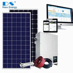
The now ready-to-assemble solar cells are tested under simulated sunlight conditions and then classified and sorted according to their efficiencies. This is handled by a solar cell testing device that automatically tests and sorts the cells. The factory workers then only need to withdraw the cells from the respective efficiency repository to which the machine assorted the cells.

The solar cell then basically becomes a new raw material that is then used in the assembly of solar PV modules. Depending on the smoothness of the production process and the basic silicon wafer material quality, the final outcome in form of a solar cell is then further graded into different solar cell quality grades.
Peripheral equipment and conditions
Peripheral equipment in the production process of battery, power supply, water supply, drainage, hvac, vacuum, special steam and other peripheral facilities are needed. Fire protection and environmental protection equipment are also important to ensure safety and sustainable development.
A solar cell production line with an annual capacity of 50MW, only the process and power equipment power consumption is about 1800KW. The amount of process pure water is about 15 tons per hour, and the water quality is required to meet the ew-1 technical standard of China's e-grade water GB/ t11446.1-1997. The cooling water consumption of the process is about 15 tons per hour, the particle size in the water should not be more than 10 microns, and the water supply temperature should be 15-20℃. Vacuum discharge is about 300M3/H. It also requires about 20 cubic metres of nitrogen and 10 cubic metres of oxygen. Considering the safety factors of special gases such as silane, it is necessary to set up a special gas interval to ensure the absolute production safety. In addition, silane combustion tower and sewage treatment station are also necessary facilities for cell production.