
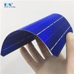


Polycrystalline silicon is composed of many small single crystals arranged in a nondirectional fashion, so many of its basic properties are the same as those of monocrystalline silicon. The main difference is that there are grain boundaries between single crystal particles in polycrystalline silicon, and there are often many amorphous silicon atoms and impurity atoms in the grain boundaries.
In the grains adjacent to the grain boundary, there are also more dislocations, defects, stresses and strains, making the life of photogenerated carriers generated by human emission light in polysilicon relatively short. Therefore, the compound current in polysilicon solar cells is large, and the open-circuit voltage, short-circuit current, filling factor and efficiency are not as high as those in monocrystalline silicon cells.

And the general photoelectric special ~10 kinds of silicon band technology in the study, there are four more mature, namely: (1) edge feeding film method (EFG); (2) jumping dendrite method (DB); Silicon cylinder method (SB); (4) electric spray method. The silicon with a thickness of about 200 materials m obtained by these four methods. When viewed along the growth direction of silicon with a uniform crystal orientation, and when viewed along the direction of bandwidth, the crystal direction is more complex, so it is often called that the silicon with a fibrous crystal structure is semicrystalline silicon. Solar cells made from semi-crystalline silicon wafers have achieved an average efficiency of more than 10 percent, and some have reached 15 percent.
Among them: (1) edge feeding film method, is to use the graphite mold engraved with the slit immersion in silicon melt, by capillary phenomenon, the liquid silicon along the slit up, with the seed silicon wafer silicon liquid along the slit condensation upward stretch, that is, with equal width and thickness of silicon band; (2) the leap-like dendrite method USES two fine seed crystals to extend into the silicon melt in parallel, and the silicon liquid forms a webbed lunar-like silicon film between the seed crystals by means of surface tension, and lifts the seed crystal upward. (3) silicon cylinder method, is to use the width of about 125 mm, thickness of about 0.2 mm of 9 pieces of seed crystal, surrounded by 8-sided shape, extend the silicon melt, and then pull up, you can get an 8-sided shape of silicon cylinder, with laser segmentation, you can get uniform thickness, better quality of silicon. Due to the rapid growth of silicon tube and low chip loss, the efficiency of solar cells made from silicon tube substrates has reached 12%~14.5%. (4) electronic spray method, is by the polycrystalline silicon powder electronic spray to high temperature substrate, forming a width of 60cm, several meters long, can be wound polycrystalline silicon band. The typical parameters of photovoltaic modules made of this electronic spray polycrystalline silicon strip material are: output power resin. GV, geometric dimension (LxwxH) -1633mm pie 660mmx35mm (5) solar grade silicon: it is generally considered a cheap type of silicon capable of producing solar cells with an efficiency of more than 10%.
Methods are being developed to prepare solar grade silicon from a fluidized bed reactor and direct purification of metallurgical silicon. The high purity granular polycrystalline silicon produced from the boiling bed reactor catalyzed by zinc has been used as raw material for silicon solar cells. The properties and manufacturing process are the same as those of monocrystalline silicon solar cells. Because pulling monocrystalline silicon requires a lot of energy and the high cost of high purity quartz increases the risk, people began to explore the use of polysilicon as the material for making solar cells in the 1960s. Which mainly include: (l) thin film polysilicon: in cheap substrate, such as metallurgical silicon that metals), graphite, ceramics, using chemical vapor deposition method (VCD), such as ion enhanced chemical vapor deposition method (PCDV) and metal organic chemical vapor deposition method (M (X 2 VD), grow a layer of polycrystalline thin layer of 20 ~ 50 mix M, hence made of polycrystalline silicon solar cell efficiency has more than 10. (2) ingot polysilicon: molten silicon is cooled directionally by graphite vortex increasing to obtain polysilicon ingot with longitudinal arrangement of grain boundary and large grain size, which is cut by multi-line cutting machine or inner circle cutting machine. 2~ 0.4m thick large area polycrystalline silicon wafers. The efficiency of the polycrystalline silicon solar cell made from this has reached 17%~18. Compared with the pulled monocrystalline silicon, this ingot silicon has short production cycle, large production t (up to 240 kg for a single ingot) and low price.