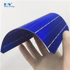


Directional solidification mono like solar wafer is one of the promising alternative wafer materials compared with monocrystalline silicon wafer and multicrystalline silicon wafer due to its relatively higher conversion efficiency and lower production cost. But there is still a large room to improve the crystal quality and to reduce the manufacturing cost, which could push the wafers into photovoltaic industry practically.
1Material properties
|
Property |
Specification |
Inspection Method |
|
Growth method |
directional solidification |
XRD |
|
Crystallinity |
Monocrystalline |
Preferential Etch Techniques(ASTM F47-88) |
|
Conductivity type |
P-type |
Napson EC-80TPN P/N |
|
Dopant |
Boron,Gallium |
- |
|
Oxygen concentration[Oi] |
≦1E+17 at/cm3 |
FTIR (ASTM F121-83) |
|
Carbon concentration[Cs] |
≦1E+18 at/cm3 |
FTIR (ASTM F123-91) |
2Electrical properties
|
Property |
Specification |
Inspection Method |
|
Resistivity |
0.5-2 Ωcm (After anneal) |
Wafer inspection system |
|
MCLT (minority carrier lifetime) |
≧10 μs |
Sinton QSSPC |
3Geometry
|
Property |
Specification |
Inspection Method |
|
Geometry |
Square or Rectangle |
Wafer inspection system |
|
Bevel edge shape |
Line |
Wafer inspection system |
|
Wafer size (Side length*side length) |
156mm*156mm 157mm*186mm 166mm*166mm |
Wafer inspection system |
|
Angle between adjacent sides |
90±3° |
Wafer inspection system |
Hot Tags: p type directional solidification mono like solar wafer including 166mm*166mm, China, suppliers, manufacturers, factory, made in China