Products Introduction

Material Properties
| Prime Specifications | 6" | 8" | 12" |
| Growth Method | CZ | CZ | CZ |
| Diameter (mm) | 150±0.5 | 200±0.5 | 300±0.5 |
| Type/Dopant: | P/Boron or N/Ph | P/Boron or N/Ph | P/Boron or N/Ph |
| Thickness (μm) | 625±25/675±25 | 725±25 | 775±25 |
| Resistivity | 1–100Ω | 1–100Ω | 1–100Ω |
| TTV | ≤10um | ≤10um | ≤10um |
| BOW | ≤40um | ≤40um | ≤40um |
| WARP | ≤40um | ≤40um | ≤40um |
| Particle | ≤30ea@≥0.2um | ≤30ea@≥0.2um | ≤30ea@≥0.2um |
| Flat/Notch | Flats/Notch | Flats/Notch | Notch |
| Surface Finish | As-Cut/Lapped/Etched/SSP/DSP | As-Cut/Lapped/Etched/SSP/DSP | As-Cut/Lapped/Etched/SSP/DSP |
| Customized Specifications Available | |||

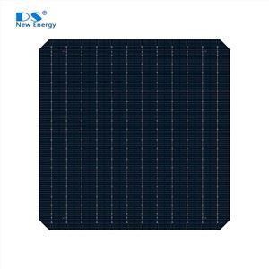
Prime wafers are manufactured to meet the highest standards required for semiconductor device fabrication. With tighter controls on TTV, BOW, warp, and particle levels, these wafers deliver superior flatness and surface quality, making them ideal for chip production and advanced process development. Whether for large-scale manufacturing or precision R&D, prime wafers provide the consistency needed to achieve top yield and performance.
Product features
Sizes Available: 6", 8", and 12"
Growth Method: CZ (Czochralski) process
Diameter Tolerance: 150±0.5 mm, 200±0.5 mm, 300±0.5 mm
Doping Options: P-type (Boron) or N-type (Phosphorus)
Thickness: 625–775 µm (depending on wafer size)
Resistivity Range: 1–100 Ω
TTV: ≤10 µm
BOW: ≤40 µm
Warp: ≤40 µm
Particle Level: ≤30@≥0.2 µm
Flat/Notch Options: Flats or Notch
Surface Finish: As-Cut, Lapped, Etched, SSP, DSP
Customizable: Tailored specifications available

Hot Tags: prime wafer, China, suppliers, manufacturers, factory, made in China