


Products Introduction

Material Properties
| Dummy Specifications | 6" | 8" | 12" |
| Diameter (mm) | 150±0.5 | 200±0.5 | 300±0.5 |
| Type/Dopant: | P/Boron or N/Ph | P/Boron or N/Ph | P/Boron or N/Ph |
| Thickness (μm) | 625±25/675±25 | 725±25 | 775±25 |
| Flat/Notch | Flats/Notch | Flats/Notch | Notch |
| Surface Finish | As-Cut/Lapped/Etched/SSP/DSP | As-Cut/Lapped/Etched/SSP/DSP | As-Cut/Lapped/Etched/SSP/DSP |

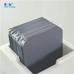
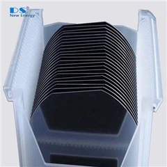
Dummy wafers are widely used in semiconductor manufacturing as a cost-effective solution for equipment calibration, process stabilization, and routine testing. Unlike product wafers, dummy wafers do not carry active circuits, but they play a critical role in ensuring that production tools run smoothly before high-value silicon wafers are processed.
Our silicon dummy wafers are available in 6-inch, 8-inch, and 12-inch sizes, with multiple options for dopants (P/Boron or N/Ph), thickness, flats or notches, and surface finishes (as-cut, lapped, etched, SSP/DSP). These specifications make them suitable for a wide range of applications, from tool qualification to process development and equipment monitoring.
By using dummy wafers, manufacturers can reduce costs, improve wafer yield, and maintain consistent quality in chip production. They are a practical choice for fabs, research labs, and semiconductor equipment maintenance.
Product features
Available Sizes: 6", 8", and 12" silicon wafers
Precise Diameter Control: 150±0.5 mm, 200±0.5 mm, 300±0.5 mm
Flexible Doping Options: P-type (Boron) or N-type (Phosphorus)
Thickness Range: 625±25 μm, 675±25 μm, 725±25 μm, 775±25 μm
Flat/Notch Options: Flats or Notch, depending on wafer size
Surface Finish: As-Cut, Lapped, Etched, SSP (Single-Side Polished), DSP (Double-Side Polished)
Cost-Effective: Ideal for equipment calibration, tool monitoring, and process testing
Stable Performance: Ensures consistent production environment before processing product wafers

Hot Tags: dummy wafer, China, suppliers, manufacturers, factory, made in China