


The fact that cell technologies featuring the highest efficiencies in industrial production are based on N type Cz-Si wafer is a striking demonstration of why n-type wafers are the most suitable material for high-efficiency solar cells. Going more into details, there are some physical reasons for the superiority of N type versus P type, the most important are:
due to absence of boron, there is no light induced degradation (LID) occurring in p-type Si wafers, due to boron-oxygen complexes
as N type Si is less sensitive to prominent metallic impurities, in general the minority carrier diffusion lengths in n-type Cz-Si are significantly higher compared to p-type Cz-Si
N type Si is less prone to degradation during high temperature processes such as B-diffusion.
1 Material properties
Property | Specification | Inspection Method |
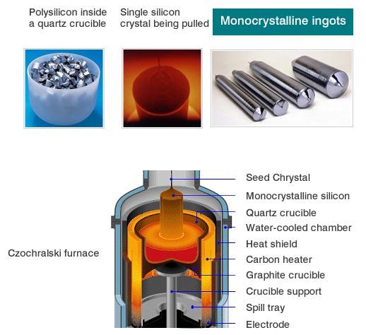
Growth method | CZ | |
Crystallinity | Monocrystalline | Preferential Etch Techniques(ASTM F47-88) |
Conductivity type | N-type | Napson EC-80TPN |
Dopant | Phosphorus | - |
Oxygen concentration[Oi] | ≦8E+17 at/cm3 | FTIR (ASTM F121-83) |
Carbon concentration[Cs] | ≦5E+16 at/cm3 | FTIR (ASTM F123-91) |
Etch pit density(dislocation density) | ≦500 cm-3 | Preferential Etch Techniques(ASTM F47-88) |
Surface orientation | <100>±3° | X-ray Diffraction Method (ASTM F26-1987) |
Orientation of pseudo square sides | <010>,<001>±3° | X-ray Diffraction Method (ASTM F26-1987) |
2 Electrical properties
Property | Specification | Inspection Method |
Resistivity | 0.2-2.0 Ω.cm 0.5-3.5 Ω.cm 1.0-7.0 Ω.cm 1.5-12 Ω.cm Other resistivity | Wafer inspection system |
MCLT (minority carrier lifetime) | ≧1000 μs(Resistivity > 1 Ωcm) | Sinton transient |
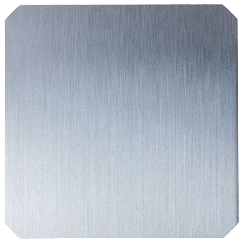
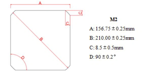
3 Geometry
Property | Specification | Inspection Method |
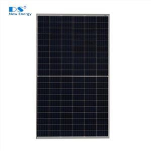
Geometry | Pseudo square | |
Bevel edge shape | Round | |
Wafer size (Side length*side length * diameter | M0: 156*156*ϕ210 mm M1: 156.75*156.75* ϕ205mm M2: 156.75*156.75* ϕ210 mm | Wafer inspection system |
Angle between adjacent sides | 90±3° | Wafer inspection system |
Hot Tags: N Type 156.75mm Monocrystalline Solar Wafer, China, suppliers, manufacturers, factory, made in China