


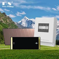
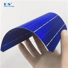
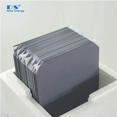
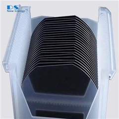


The N-Type M2 Monocrystalline Silicon Wafer features a quasi-square 156.75×156.75 mm design with rounded corners, balancing compatibility with standard module layouts and optimized light capture. Produced using the CZ method and phosphorus doping, it offers high material purity, <100> orientation, and low dislocation density (≤500 cm⁻²). With N-type conductivity, a wide resistivity range (0.2–12 Ω·cm), and high minority carrier lifetime (≥1000 µs), it supports high-efficiency cell technologies such as TOPCon and HJT. The M2 wafer remains a proven and reliable format for stable performance in mainstream PV applications.
1. Material properties
|
Property |
Specification |
Inspection Method |
|
Growth method |
CZ |
|
|
Crystallinity |
Monocrystalline |
Preferential Etch Techniques(ASTM F47-88) |
|
Conductivity type |
N-type |
Napson EC-80TPN |
|
Dopant |
Phosphorus |
- |
|
Oxygen concentration[Oi] |
≦8E+17 at/cm3 |
FTIR (ASTM F121-83) |
|
Carbon concentration[Cs] |
≦5E+16 at/cm3 |
FTIR (ASTM F123-91) |
|
Etch pit density(dislocation density) |
≦500 cm-2 |
Preferential Etch Techniques(ASTM F47-88) |
|
Surface orientation |
<100>±3° |
X-ray Diffraction Method (ASTM F26-1987) |
|
Orientation of pseudo square sides |
<010>,<001>±3° |
X-ray Diffraction Method (ASTM F26-1987) |
2.Electrical properties
|
Property |
Specification |
Inspection Method |
|
Resistivity |
0.2-2.0 Ω.cm
0.5-3.5 Ω.cm
1.0-7.0 Ω.cm
1.5-12 Ω.cm
|
4-probe resistivity
measurementt
|
|
MCLT (minority carrier lifetime) |
≥1000 µs (Resistivity>1.0 Ω.cm)
≥500 µs (Resistivity<1.0 Ω.cm
|
Sinton BCT-400
Transient
(with injection level: 5E14 cm-3)
|
3.Geometry
|
Property |
Specification |
Inspection Method |
|
Geometry |
quasi square
|
Vernier caliper
|
|
Diameter
|
210 ±0.25 mm
|
Vernier caliper |
|
Flat to flat
|
156.75 ±0.25 mm
|
Vernier caliper
|
|
Corner length
|
8.5 ± 0.5mm
|
Wide-seat square/ruler
|
|
Angularity
|
90° ± 0.2° |
Angle ruler
|
|
Corner shape
|
Round shape
|
Visual inspection
|
|
Perpendicularit
|
≤ 0.8 mm
|
|
|
TTV (Total thickness variation) |
≤ 27 µm |
wafer inspection system |

4.Surface properties
|
Property |
Specification |
Inspection Method |
|
Surface qualit
|
Stain, Oil, Scratch, Crack, Pit, Bump,
Pinhole and Twin defect are not
allowed
|
Visual inspection
|
|
Chip
|
Surface chip is not allowed;
Arris: chips are inconsecutive:
Less than 10 on the arris, dia≤0.3mm;
|
Ruler
|
|
Surface roughne
|
Plane surface : Ra≤0.6um;
Cambered surface : Ra≤1.0um
|
Surface roughness meter
|
Hot Tags: n-type m2 monocrystalline silicon wafer specification, China, suppliers, manufacturers, factory, made in China


