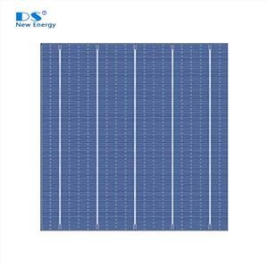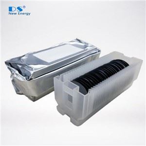


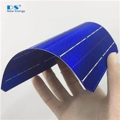
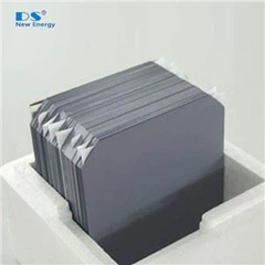
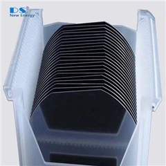


The mono-crystalline wafer production flow consists of cutting, cleaning and sorting procedures. Currently, more than 80% of the worldwide Cz-Si crystal production capacity for PV is dedicated to p type.
1 Material properties
Property | Specification | Inspection Method |
Growth method | CZ | |
Crystallinity | Monocrystalline
| Preferential Etch Techniques(ASTM F47-88) |
Conductivity type | P-type | Napson EC-80TPN P/N |
Dopant
| Boron, Gallium
| - |
Oxygen concentration[Oi] | ≦9E+17 at/cm3 | FTIR (ASTM F121-83) |
Carbon concentration[Cs] | ≦5E+16 at/cm3 | FTIR (ASTM F123-91) |
Etch pit density(dislocation density) | ≦500 cm-3 | Preferential Etch Techniques(ASTM F47-88) |
Surface orientation | <100>±3° | X-ray Diffraction Method (ASTM F26-1987) |
Orientation of pseudo square sides | <010>,<001>±3° | X-ray Diffraction Method (ASTM F26-1987) |
2 Electrical properties
Property | Specification | Inspection Method |
Resistivity | 1-3 Ωcm (After anneal) | Wafer inspection system |
MCLT (minority carrier lifetime) | ≧20 μs | Sinton QSSPC |
3 Geometry
Property | Specification | Inspection Method |
Geometry | Pseudo square | |
Bevel edge shape | Round | |
Wafer size (Side length*side length * diameter | M0: 156*156*ϕ210 mm M1: 156.75*156.75* ϕ205mm M2: 156.75*156.75* ϕ210 mm | Wafer inspection system |
Angle between adjacent sides | 90±3° | Wafer inspection system |
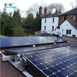
Hot Tags: P Type 156mm Monocrystalline Solar Wafer, China, suppliers, manufacturers, factory, made in China